• HOME
  • About
  • Contact Resistivity
  • Non Contact Resistivity
    • Non Contact In Line
  • PN Type Check
  • Flatness/Thickness
  • Life-Time
  • Spreading Resistance
  • Reference Wafers
  • 4 Point Probes
  • Contact Us
  • Technical Principles
Stein Labs, LLC
Search Solutions
Picture
Life-time Measurement Systems

HF-90R Life-time measurement system for silicon bulks / ingots with non-contact
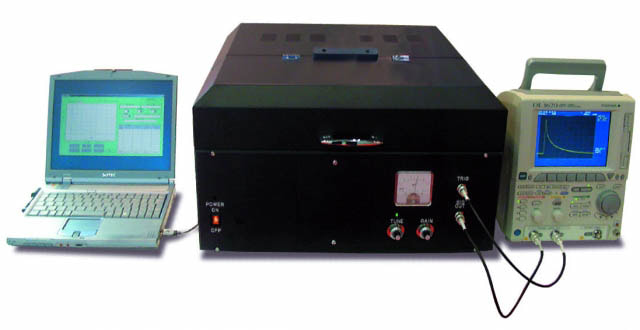
Picture
Picture
Picture
Picture
Description
​
  • Silicon bulk, Prismatic shape (JIS code), Ingot condition
  • Non-contact photoconduction vibration decay method
  • Data processing by digital oscilloscope and PC with software
Applications
  • Silicon ingot, Silicon bulk, Prismatic shape (JIS code)

Sample sizes
*Please contact us in details

Measuring range
100 ~ 5,000μS (in the range of 10 ~ 5,000Ω・cm)


HF-300 Non-contact Mono/Polycrystalline Silicon Wafer or Brick Life-time measurement


Picture
Picture
Picture
Picture
Picture
Description
  • Non-contact, non-damage measurement by μ-PCD
  • Suitable for mono-crystalline and polycrystalline silicon sample
  • Multipoint measurement & mapping image
  • Passivation with exclusive capsule (for wafer, bulk sample)

Applications
Silicon wafer, blick(bulk) [Mono-crystalline, Polycrystalline]


Sample sizes:
  • [Wafer] <Square> ~ 210x210mm, <Circle> ~8 inch
  • [Brick] Max. 210(W) x 210(H) x 500(D) mm


Measuring range:
0.1 μS ~ 1000μS (*Compatible to resistivity range ; 0.1 ~ 1,000Ω・cm)
<Laser unit> Type : Semiconductor laser diode,
Wave length : 905nm, Peak power : 60W, Pulse width : 80nS


Related product
​
Inline lifetime measurement module : HF-300BI

HF-100DCA Life-time measurement system for Silicon bulks/ingots-JIS Method

Picture
Picture
Picture
Picture
Description
  • Global standard model for the lifetime test of silicon bulk
  • JIS direct current anodizing method
    Data processing by digital oscilloscope and PC with software

Applications
  • Silicon ingot, Silicon bulk, Prismatic shape (JIS code)

Sample sizes: Please contact us in details

Measuring range: 50 μS~ 20mS


HOME   
CONTACT RESISTIVITY
NON-CONTACT RESISTIVITY
FLATNESS/THICKNESS
P/N TYPING
NON-CONTACT IN-LINE
LIFE TIME
SPREADING RESISTANCE
4 POINT PROBE HEADS 
TECHNICAL PRINCIPLES
NRW REFERENCE WAFERS
ABOUT
CONTACT US
© 2022 Stein Labs, LLC. & Napson Corporation  All rights Reserved.  Bedford, MA    PHONE: +1 (508) 591-3686  EMAIL: