• HOME
  • About
  • Contact Resistivity
  • Non Contact Resistivity
    • Non Contact In Line
  • PN Type Check
  • Flatness/Thickness
  • Life-Time
  • Spreading Resistance
  • Reference Wafers
  • 4 Point Probes
  • Contact Us
  • Technical Principles
Stein Labs, LLC
Search Solutions

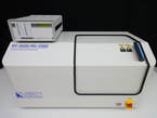
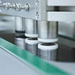
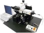
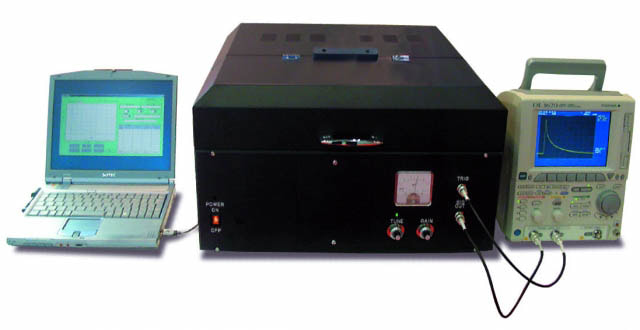
Inspection & test equipment
semiconductor, solar, thin film applications.


Stein Labs is pleased to offer solutions for batch, roll to roll automation, bench top equipment for Semiconductors, thin films, epi wafers,nano-tech from
Picture
Please select your product of interest below, or see our "Contacts" page for a more detailed request. 

Picture
Contact Resistance Probe measurement
  • 4-point (or 2-point) probe head to contact the sample for the measurement.
  • Widest measurement range
  • Suitable for various materials.
Picture
Non Contact Resistance measurement
  • Paired eddy-current probe heads for measurement
  • No damage to the measurement surface
Picture
​Flatness/Thickness measurement
  • Wafer flatness(TTV, BOW, WARP) & thickness 
  • No damage to the surface 
Picture
PN Type Check
Tests for P or N Type using either the Photoelectric or Seebeck Effect
Picture
Spreading Resistance
​Spreading Resistance Measurement System using slant polished substrates​

​
Picture
Lifetime measurement
  • Accurately measure carrier life-times 
  • Models for wafers, ingots, bulk, prismatic Silicon
Picture
4 Point Probe 
​(Head Only)
  • Jandel Jeweled probe heads
Picture
​NRW Resistivity
​Reference Wafers
  • Accurately calibrated wafer standards
  • Complies with SEMI, JIS, ASTM Standards
HOME   
CONTACT RESISTIVITY
NON-CONTACT RESISTIVITY
FLATNESS/THICKNESS
P/N TYPING
NON-CONTACT IN-LINE
LIFE TIME
SPREADING RESISTANCE
4 POINT PROBE HEADS 
TECHNICAL PRINCIPLES
NRW REFERENCE WAFERS
ABOUT
CONTACT US
© 2020 Stein Labs, LLC. & Napson Corporation  All rights Reserved.  Bedford, MA    PHONE: +1 (508) 591-3686  EMAIL: 
info@steinlabs.com